SANTA CLARA, Calif. — The high-bandwidth-memory market has become one of the biggest beneficiaries of the artificial-intelligence boom. Every new generation of accelerator has required more HBM capacity, more stacks and more advanced packaging, turning memory into a critical — and increasingly expensive — part of the AI system. PhantaField is proposing a more disruptive answer: remove HBM from the accelerator altogether.
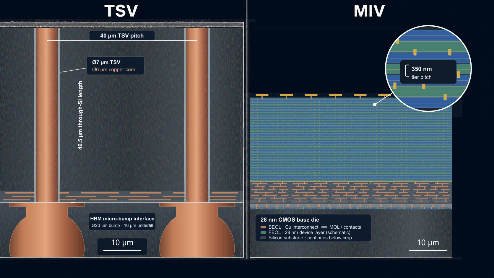
The company's Sophon PFG-1 reference design uses monolithic 3D integration to grow memory and logic tiers directly above a mature 28 nm CMOS base. Its 80-tier architecture interleaves 40 logic tiers with 40 memory tiers and places 330 GB of capacitor-less 2T0C gain-cell DRAM inside a pure-digital compute-in-memory fabric. Instead of fetching model weights from HBM stacks across an interposer, Sophon keeps the weights in the tiles that perform the arithmetic.
A direct challenge to HBM's role in AI accelerators
That distinction matters because HBM is more than a memory product: it is the organizing principle of today's accelerator package. GPU designers allocate die-edge bandwidth, interposer area, power and a large share of system cost around it. PhantaField's architecture removes those constraints in one move. The PFG-1 design targets 2.10 PB/s of in-tile weight bandwidth — roughly 100 times the bandwidth of an eight-stack HBM4 package — while holding an entire 80-billion-parameter model on one die.
If those targets are validated in silicon, the competitive question for accelerator vendors changes. The issue would no longer be which supplier can deliver the fastest HBM stack, but whether a workload needs external high-bandwidth memory in the first place. That could reduce the number of HBM stacks required per inference system, weaken the link between AI-compute growth and HBM volume, and shift more value from memory packages toward integrated memory-compute architectures.
HBM wins by widening the road between memory and compute. Sophon changes the market by eliminating the trip.
PhantaField
Inference is the first pressure point
The most immediate exposure is low-batch generative-AI inference. In that workload, each new token requires the accelerator to read a large share of the model's weights, leaving expensive compute units waiting on memory bandwidth. Sophon's modeled targets for an 80B model — 14,438 FP8 tokens per second at batch one and 25.8 millijoules per token at die level — come from keeping those weights resident inside the compute array rather than repeatedly moving them across a package.
On PhantaField's thesis, HBM demand does not merely shrink — it disappears. The sequence runs through the workloads: low-batch inference first, where the economics are most lopsided and every token pays the memory toll; then training, once vertical density puts the full working set on-die; and finally the general-purpose accelerator itself, as software ecosystems migrate. The barrier that historically made such transitions slow — the installed toolchain, the CUDA moat, years of hand-ported kernels — has already been broken by AI coding: models now translate kernels, generate compiler backends and port serving stacks in weeks rather than engineering-years, so software lock-in no longer protects incumbent hardware the way it protected it for two decades. Once memory can be grown inside the processor for less than it costs to buy beside it, the discrete memory package becomes a legacy interface.
Vertical density: how 28 nm can out-build 3 nm
The deeper reason Sophon needs no HBM — even for training — is what monolithic stacking does to transistor density. Because each tier is grown directly on top of the last rather than bonded, compute layers stack the way memory layers do in 3D NAND: density scales vertically instead of through ever-finer lithography. Thirty-two logic tiers built at mature 28 nm geometry put more transistors above a square millimeter of silicon than a single-layer 3 nm die — so a process node from 2011, multiplied through the third dimension, can exceed the effective density of the most advanced planar node money can buy, without EUV and without leading-edge wafer allocation.
That vertical density is what breaks HBM's last stronghold: training. The workload long assumed to be permanently tied to external memory fits entirely on one die, because 330 GB of on-die DRAM holds the full training working set — an 80-billion-parameter BF16 model, its optimizer state and activations — with gradients written back into the same cells at 20 femtojoules per bit. The whitepaper models 2,406 training tokens per second at a 472 W average, and at gigawatt fleet scale reaches training-time parity with HBM4 GPU fleets at roughly 2.9 to 3.7 times lower hardware cost. In this architecture, training does not need HBM at all — the memory it would have bought is grown into the processor instead.
A new strategic problem for memory suppliers
For HBM manufacturers, PhantaField creates both a threat and an option. The threat is demand avoidance: every accelerator that keeps its model on-die is an accelerator that does not need multiple premium HBM stacks. The option is to move closer to the architecture PhantaField is describing — investing in custom base dies, logic-on-memory, 3D DRAM and tighter integration with compute. In that sense, Sophon could accelerate a transition already visible in the market, from selling standardized memory stacks toward co-designing workload-specific memory systems.
Advanced packaging would feel the same pressure. HBM-based accelerators depend on silicon interposers, thousands of package-level connections and a complex multi-die supply chain. A monolithic-3D device that grows memory over logic could redirect value toward low-temperature deposition, inter-tier vias and back-end process equipment. PhantaField's NanoGalaxy PP-MOCVD platform is central to that strategy: it targets wafer-scale 2D semiconductor growth below 450 °C, a thermal budget intended to make additional transistor tiers compatible with finished CMOS.
The proof point is silicon, not a specification sheet
The potential market impact is substantial, but it is not yet assured. PFG-1 is a reference design at the tape-out stage, and its bandwidth, throughput, energy and cost figures are modeled engineering targets rather than measured results from a shipping product. PhantaField must demonstrate the 2T0C cell's retention and variability, reliable 80-tier integration, acceptable yield on a large die, and a software stack that lets customers deploy models without abandoning familiar workflows.
That makes the near-term shock to HBM strategic rather than financial. Sophon gives accelerator companies, hyperscalers and memory vendors a credible new question to plan around: what happens when AI memory stops being a component beside the processor and becomes part of the processor itself? If PhantaField closes the gap between its model and manufactured silicon, the answer is an AI accelerator market that stops buying memory as a separate component at all — and a much faster race to build the architectures that come after it.