You order HBM4 for your next GPU, and the allocation comes back short. Customers reportedly get 60–70% of what they order. Put a ruler against a stack that does arrive, and it stands 775 µm tall. Inside are twelve or sixteen thinned DRAM dies on a base die. Wires run through holes drilled in the silicon, and each die is bonded to the next.
Today we’re introducing Van der Waals, a 3D DRAM we grow one layer at a time, and publishing the whitepaper behind it. We want every GPU to carry more memory, from wafers HBM doesn’t draw on.
Why there isn’t enough HBM
HBM is hungry for wafers, and by the end of this year it’s expected to take about 22% of DRAM wafer input. In return it makes about 9% of the bits. And every time HBM adds a layer, it needs a thinner die, one more bond or a taller package.
Each layer, which we call a tier, is 0.35 µm thick. A stack has 48 of them. Together they’re 16.8 µm, thinner than a sheet of paper. We grow them with our own tool, NanoGalaxy, on our own silicon or on the GPU wafer itself.
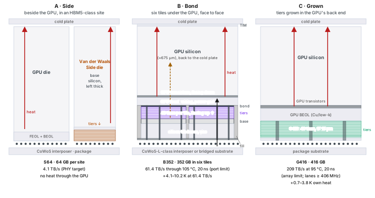
The memory comes three ways. Side fills one HBM site, the spot beside the GPU where a stack sits, with 64 GB. Bond puts 352 GB under each GPU die. Grown puts 416 GB inside it.
Every gigabyte we grow is one that never had to come out of an HBM allocation.
PhantaField
You’re buying at the top of the market
Conventional DRAM contract prices rose 93–98% in the first quarter of this year alone. HBM is sold on yearly contracts, so its price has moved less. DDR5 on the spot market now costs more than HBM3E’s $12.0–12.8 per GB.
We won’t sell you Van der Waals on dollars per GB. In the next downturn, DIMMs would sell for less than it costs us to make. Side costs us $8.52 a GB to make. Bond comes to $10.62. Grown works out at $8.28–8.45, counted over good GPUs only. That is cost, not price. Side and Grown cost about 1.3 times our estimate of HBM’s cost. For Bond it’s 1.6 times.
Against a market at its peak, we add bits that don’t come from DRAM wafers. Bond also gives a GPU die 2.4× the memory a current flagship die gets from HBM4.
Sixteen dies that all have to work
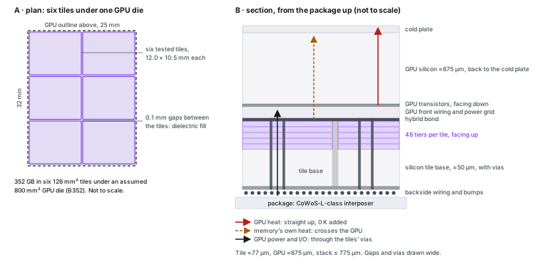
An HBM stack is good only if every die and joint in it is good, so we keep our pieces small. Side’s die and each Bond tile are 126 mm², about the size of a fingernail. At the defect density we design to, silicon that size yields 88.28%. A die the size of a big GPU yields only 47.38%.
Each tier must also grow clean, and published figures for chips built layer by layer give us the odds. Side’s die and each Bond tile then yield 76.4% before any spare is used. Each stack carries 2 spare tiers to stand in for one that fails.
We test each die and tile before it meets the GPU, so a bad Side die never costs you a GPU. In Bond, a failed bond or a power short in a tile scraps the GPU. Grown’s tiers go onto untested GPUs, where a power short does the same.
Hot memory forgets faster
DRAM leaks its charge faster as it warms, so it must refresh more often. From 85 to 95 °C, DDR5 refreshes twice as often. An HBM stack puts all its thinned dies in its heat path, and as many bonded joints.
Our tiers have no bonded joint between them, so a Side die’s memory runs within 0.5–1 K of its base. All three formats are rated with the memory as hot as 105 °C. Ours still refreshes more when hot, and at that heat Bond spends about twice the highest refresh power HBM lists.
Moving bits makes heat too. HBM4 spends 2.4–4 pJ, or picojoules, to move a bit. Bond moves a bit from its cell to the GPU’s receiver for 0.08–0.4 pJ, not counting the logic in its base. Its bit crosses one bond. HBM’s crosses millimeters of package wiring and two sets of edge circuits, one on the GPU and one on the stack’s base die. Edge circuits are what let one chip talk to another. So Bond spends 6 to 48 times less energy per bit.
Bond’s own heat crosses the GPU to reach the cold plate. Run it at 22 TB/s, what a current flagship GPU moves across its two dies. The GPU’s transistors then run +1.3–4.0 K warmer. Bond’s base logic and leakage can push that to +8.6 K. At full speed, the rise is +4.1–10.2 K.
How fast each gigabyte reads
HBM4 gives 57–92 GB/s for each GB it holds. A current flagship GPU die gets 144 GB of it. It reads that memory at 11 TB/s.
Memory under the GPU reads faster. Bond moves 61.4 TB/s per GPU die. It keeps that pace with its memory as hot as 105 °C. A current flagship die would need 5.6 times its HBM4 bandwidth to match. Spread over Bond’s memory, each GB gets 175 GB/s.
Grown is faster again, at 209 TB/s per GPU die. It gets there with its memory at 95 °C. Each GB it holds gets 503 GB/s.
Bandwidth is Side’s concession. With the edge circuits we aim for, it gets 4.1 TB/s per site. Each GB gets 64 GB/s. Vendors already sell edge circuits for the 28 nm process we priced the die on. They’re slower, and give Side 2.2 TB/s. Either way, each GB gets less than HBM5 will give, however you read what one HBM maker has said. Side suits work that needs room more than speed, like key-value caches and long context.
One more thing, for space
A cosmic ray flips a bit by dumping charge into it. Our channel is a single layer of atoms. The bit sits on a transistor gate, not in a trench capacitor. A particle passing through finds almost nothing to deposit charge in. That is what makes a memory radiation hard, and it is why we expect Van der Waals to fly. No part has been irradiated yet, so the soft-error rate is still to be measured. If you are building compute for orbit, ask us about it.
Three ways to get it
All three use the same tiers, built in MoS₂, a semiconductor grown in sheets a few atoms thick. Each bit is a charge on one transistor’s gate, read through a second with no capacitor, which makes it a 2T0C gain cell.
Side (S64) is one tested die for an HBM5-class site. It stands as tall as an HBM stack, with no wires drilled through it and no stacked dies. Side needs a GPU with an HBM5-class controller, though HBM5 itself isn’t published yet.
Bond (B352) is six tested tiles, bonded face to face under each GPU compute die with no solder bumps between them. The GPU keeps its silicon back against the cold plate. Its power and signals run down through wires inside the tiles.
Grown (G416) is a process the GPU maker’s foundry runs on the GPU wafer, the dinner-plate disc the GPUs are cut from. It grows 48 tiers between the GPU’s top layer of wiring and its solder bumps. Nothing is bonded or drilled, and no edge circuit sits in the way. We supply the process, the growth tools and a design kit.
Who should call
Van der Waals is for GPU makers, their foundries and the clouds that buy the GPUs. The whitepaper carries every calculation and sources the market figures. Send your GPU’s HBM sites, die face, power map and process flow through the contact form, and we’ll tell you which format fits.
We’ve measured the material, the MoS₂ transistors and a 2T0C cell with a MoS₂ write transistor over a silicon read transistor. The all-MoS₂ cell every tier needs is modeled from those results. So are the capacity, bandwidth, heat, yield, cost and energy figures in this post. We haven’t yet built a bonded part or grown tiers on a GPU, and no failed tier has been switched out for a spare.
Don’t ask how many stacks you’ll be allocated.
Ask how much memory we can grow for each GPU.
Frequently asked questions
- Does Van der Waals cost less than HBM?
- No. Side and Grown cost us about 1.3 times our estimate of HBM’s cost per GB. For Bond it’s 1.6 times. Putting the memory beside, under or inside the GPU moves cost and risk around. It doesn’t lower what a bit costs. Our case rests on supply and capacity, and for Bond and Grown on bandwidth per GB.
- Does it replace HBM?
- Side can. It fills an HBM5-class site with 64 GB from one tested die, for capacity more than speed. Bond and Grown add memory under or inside the GPU die, closer than any HBM stack can sit. In exchange they add some heat at the GPU’s transistors.
- What does my GPU have to change?
- For Side, you need an HBM5-class controller, and edge circuits that can talk to a 64 GB die. For Bond, your die must take its power from the front. Where its bumps would be, it needs the pads and memory ports our tiles bond to. Grown needs front power too, and a grid for the towers that carry power and signals through the tiers. It also needs the receivers and controllers the memory talks to, and a foundry to qualify the process. Our bond follows the open UCIe-3D class of links between stacked dies, so any GPU or accelerator maker can build to it.
- What if a tier, tile or die fails?
- Each stack carries two spare tiers to stand in for a tier that fails, and Grown counts on them. Side is tested before it meets the GPU, so a bad die never costs you a GPU. Bond tiles are tested too, and a tile whose memory fails after bonding can be mapped out and left unused. In Bond, a failed bond or a short in a tile’s power path scraps the GPU. In Grown, a power short through the tiers does.